Overview of FPGA design
FPGA: FPGAs are more widely used than we imagine because there are more kinds of integrated modules than just the original simple logic unit (LE). Early FPGAs were relatively simple, and all functional units were built only from pins, internal buffer, LE, and RAM, LE consisted of LUT (lookup table) and D flip-flop, and RAM also tended to have very small capacity. Nowadays, FPGAs not only include the previous LE. RAM is also larger, faster, and more flexible, the IOB is also more complex and supports more IO types, and also integrates some special functional units, including the following units. FPGA includes many series such as Zynq-7000 SoC, FPGA Spartan-7, Artix-7 FPGA, Virtex-7 FPGAs, Kintex-7 FPGAs, Virtex-6 FPGA, Spartan 6 FPGAs, and so on.
CPU core: CPU cores come in two varieties: softcore and hardcore. A soft core is an extremely flexible CPU module that is written in logic code and may be implemented in any FPGA with enough resources. A large-capacity FPGA can also incorporate numerous soft cores to enable multi-core parallel computing. The hardcore, a CPU core built inside a particular FPGA, has the benefit of speed and performance, but it is not sufficiently versatile.
SERDES: A quick serial interface. Future technology will see an increase in high-speed serial interfaces like PCI-E, XAUI, HT, and S-ATA. Without the need to buy specialized interface chips, the SERDES module allows FPGAs to quickly integrate these high-speed serial ports.
DSP: The multiplier is what it really is. While the typical DSP chip typically only has one multiplier per core, FPGA can combine several multipliers. In other words, many DSP core functions can be implemented more readily on FPGAs. The speed of numerous multiplicators operating in parallel can, in some circumstances where a lot of multiplication and addition calculations are needed, be significantly faster than the speed of a single high-speed multiplicator. Want to see more information and part number about FPGA? You can visit Vemeko FPFA to get familiar with them and if you have any demand, you can buy them.
Four main points of FPGA design
l The clock tree
l FSM
l Latch
l Logic simulation
The clock tree
Asynchronous design should be minimized when using FPGAs and should be replaced with synchronous design whenever possible. The clock tree is both the first and most important key in synchronous design. For FPGA design, a flawed clock tree is an unstoppable catastrophe, equivalent to a structure lacking a solid foundation whose unavoidable collapse. Several particular design elements:
- When possible, only use one clock.
- You must properly divide yourself into different time domains if there are any.
- The clock signal must perform synchronization processing. You can utilize double sampling for the control signal and asynchronous fifo for the data signal. Asynchronous FIFO is a useful tool, but it's not perfect. Only a specific range of frequency difference problems can be resolved by an asynchronous FIFO.
- utilizing the inherent PLL and DLL of the FPGA as much as you can improve your design greatly.
- You must carefully calculate Tsu, Tco, and Th for special IO interfaces, as well as employ PLL, DLL, DDIO, pin settable delays, and other tools. On the pins Tsu, Tco, and Th, simple limitations are frequently impossible.
FSM
Finite State Machine (FSM). The foundation of logic design can be considered to be this. The two types of FSM are the Moore type and the Marly type. Variables and Moore-type state migration are not connected; merely type is. Variable migration has nothing to do with the Moore type, but everything to do with the Marly type. In actuality, the mere type is preferred. FSM can be written in one of two ways: single-process or dual-process.
FSM appears straightforward and uncomplicated, and you are not required to include all signal and status signal processing in each case branch or if branch. For counting, you could also just add some counters to it. The compiler typically optimizes the asynchronous logic the best because synchronous and asynchronous are combined. Single-process FSMs that combine synchronous and asynchronous operations frequently provide slow logic and high resource usage due to poor compiler optimization.
Latch
Let's talk about how to avoid the harm of latch.
- In the combined logic process, if statements must have else! And all signals should be assigned in all branches of if.
Also, note that the following also generates latches. This means that the combinatorial logic process cannot assign itself to itself or indirectly assign itself to itself.
However, if it is a temporal logic process, the problem does not exist.
2) The default of the case statement must not be omitted.
3) Combination logic process sensitive variables can not be less or more.
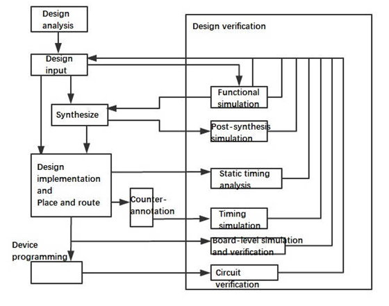
Logic simulation
The three types of simulation are system simulation, integrated simulation, and unit simulation.
Simulating each of the smallest basic modules as a unit. Code line coverage, conditional branch coverage, and expression coverage all need to be 100% for unit simulation. The COMPILE option must be selected while constructing the module in order to observe all three coverage rates.
Integrated simulation: For simulation, group multiple sizable modules together. The level of coverage is as great as it can be.
System simulation: Combined simulation of the hardware system as a whole. In this instance, the entire simulation platform consists of BFM, Testbench, and a simulation model of the logic peripheral chip interface. In order to simulate a system, simulation test cases and simulation test platforms must be carefully designed in accordance with the functional and performance requirements of the logic being emulated. System simulation is a significant subfield of logic design that necessitates in-depth investigation.